Monday, December 13, 2010

5 band graphic equalizer using a single IC/chip


This circuit uses a single chip, IC BA3812L for realizing a 5 band graphic equalizer for use in hi-fi audio systems. The BA3812L is a five-point graphic equalizer that has all the required functions integrated onto one IC. The IC is comprised of the five tone control circuits and input and output buffer amplifiers. The BA3812L features low distortion, low noise, and wide dynamic range, and is an ideal choice for Hi-Fi stereo applica-tions. It also has a wide operating voltage range (3.5V to 16V), which means that it can be adapted for use with most types of stereo equipment.

The five center frequencies are independently set using external capacitors, and as the output stage buffer amplifier and tone control section are independent circuits, fine control over a part of the frequency bandwidth is possible, By using two BA3812Ls, it is possible to construct a 10-point graphic equalizer. The amount of boost and cut can be set by external components.

The recommended power supply is 8V, but the circuit should work for a supply of 9V also. The maximum voltage limit is 16V.

The circuit given in the diagram operates around the five frequency bands:

  • 100Hz
  • 300Hz
  • 1kHz
  • 3kHz
  • 10kHz

Sunday, June 27, 2010

digital clock circuit diagram

Voltage Regulator (13.6 volts)

Clock Timer Circuit

Clock Display Circuit

Basic Clock Circuit

digital clock circuit diagram from www.bowdenshobbycircuits.info

This is a combination digital clock timer and solar panel charge controller used to maintain a deep cycle battery from a solar panel. The timer output is used to control a 12 volt load for a 32 minute time interval each day. Start time is set using 9 dip switches and ends 32 minutes later. The 32 minute duration is set by selecting the 5th bit (2^5 = 32) of a 4040 binary counter (pin 2). The timer also has a manual toggle switch so the load can be manually switched on or off and automatically shuts off after 32 minutes. The time duration can be longer or shorter (8,16,32,64,128,256 minutes etc.) by selecting the appropriate bit of the counter. The timer circuit is shown in the lower schematic just above the regulator.

The basic clock circuit (top schematic below) is similar to the binary clock (on another page) and uses 7 ICs to produce the 20 digital bits for 12 hour time, plus AM and PM. A standard watch crystal oscillator (32,768) is used as the time base and is divided down to 1/2 half second by the 4020 binary counter. One half of a 4013 data latch is used to divide the 1/2 second signal by 2 and produce a one second pulse that drives the seconds counter (74HC390 colored purple). The minutes are advanced by decoding 60 seconds (40 + 20) and then resetting the seconds counter to 0 and at the same time advancing the minutes counter. The same procedure is used to advance the hours. The second half of the 4013 latch is used to indicate AM or PM and is toggled by decoding 13 hours and resetting the hours to 0 and then advancing the hours to "one".

The clock display circuit is shown in the second drawing below and uses 6 more ICs to decode the binary data and drive four seven segment LED displays. The 10s of hours digit is driven with a single 3904 transistor. Two multiplexer circuits (4053) are used to manually select either minutes or seconds for the right two display digits. The two switches shown between the 4053s and below the left 4053 are both part of one DPDT switch which selects either seconds or minutes for the 1X and 10X digits. This switch is shown in the seconds position and the hours digits are blanked with a low signal on pin 4 of the 4511. The display can also be toggled on and off (totally blank) using a set/reset latch made from a couple 74HC00 NAND gates. A momentary DPDT switch is used to control the latch and toggle the display on or off. The second pole of this switch is used on the upper drawing (connected to the run/stop switch) to set the hours and minutes. Thus this same switch performs both functions of blanking the display and setting the time. The run/stop switch is shown in the normal running mode and supplies a low signal to a NAND gate which prevents accidental setting the time while the clock is running. The run/stop switch also turns on the display (through the diode D2) when in the stop position. The procedure for setting the clock would be to set the (run/stop) switch the stop position and the (seconds/minutes) switch to the minutes position. Then toggle the momentary switch to set minutes and hours of the current time plus one minute. The clock can then be started with the run/stop switch at precisely the right time (+/- 0.5 seconds).

The voltage regulator in the lower drawing maintains the battery at 13.6 volts and also supplies the clock and timer circuits with 4.3 volts. The charge LED indicator only comes on when the regulator is supplying max charge to the battery. When the battery voltage reaches 13.6 the regulator reduces the current to whatever is necessary to maintain the voltage and the charge indicator will turn off. The unit I built also included a battery condition indicator (voltmeter using 4 LEDs) to indicate the battery condition so that a failure of the regulator would be indicated by the charge indicator LED turned off and less than 4 LEDs lit on the voltmeter. The 4 LED battery condition indicator is shown on another page.

Sunday, June 20, 2010

32.768 KHz oscillator using a watch crystal


Below are a couple circuits you can use to produce a 32.768 KHz square wave from a common watch crystal. The output can be fed to a 15 stage binary counter to obtain a 1 second square wave. The circuit on the left using the 4069 inverter is recommended over the transistor circuit and produces a better waveform. The single transistor circuit produces more of a ramping waveform but the output swings the full supply voltage range so it will easily drive the input to a CMOS binary counter.


http://www.bowdenshobbycircuits.info

monostable multivibrator tutorial

Monostable

The monostable has only one permanent stable state.

When triggered by an external pulse, it changes over to an unstable state for a time determined by a CR time constant.

It then reverts to its stable state and waits for another trigger pulse.

OPERATION
At switch on, Tr1 is forward biased by R3.

This turns Tr1 hard on, giving it a high collector current and a low collector voltage.

This low collector voltage is cross connected to the base of Tr2, turning Tr2 off.

This is the stable state.

A negative pulse to the base of Tr1 turns Tr1 off.

The collector voltage of Tr1 goes high and turns Tr2 on.

The circuit is now in the unstable state.

C1 now charges from the supply rail via R3.

Eventually the voltage on the left hand side of C1 will be high enough to turn Tr1 back on, which in turn switches Tr2 off.

The circuit is now back in its stable state.

The monostable can be used as a short duration timer or a pulse width stretcher.

Low Frequency Sinewave Generator circuit


The two circuits below illustrate generating low frequency sinewaves by shifting the phase of the signal through an RC network so that oscillation occurs where the total phase shift is 360 degrees. The transistor circuit on the right produces a reasonable sinewave at the collector of the 3904 which is buffered by the JFET to yield a low impedance output. The circuit gain is critical for low distortion and you may need to adjust the 500 ohm resistor to achieve a stable waveform with minimum distortion. The transistor circuit is not recommended for practical applications due to the critical adjustments needed.

The op-amp based phase shift oscillator is much more stable than the single transistor version since the gain can be set higher than needed to sustain oscillation and the output is taken from the RC network which filters out most of the harmonic distortion. The sinewave output from the RC network is buffered and the amplitude restored by the second (top) op-amp which has gain of around 28dB. Frequency is around 600 Hz for RC values shown (7.5K and 0.1uF) and can be reduced by proportionally increasing the network resistors (7.5K). The 7.5K value at pin 2 of the op-amp controls the oscillator circuit gain and is selected so that the output at pin 1 is slightly clipped at the positive and negative peaks. The sinewave output at pin 7 is about 5 volts p-p using a 12 volt supply and appears very clean on a scope since the RC network filters out most all distortion occurring at pin 1.


ref:http://www.bowdenshobbycircuits.info

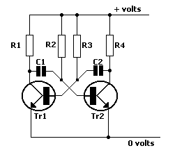
astable multivibrator tutorial

Astable

The astable has two unstable states, being unable to rest in a fixed state.

When you first switch on, one transistor is on (conducting) and the other is off (non conducting).

They stay in this unstable state for a time, determined by a CR time constant.

Then the transistors exchange states, the one that was off coming on, and the one that was on going off.

They stay in this new unstable state for a time, again determined by a CR time constant, before reverting to the original state.

This process is repeated continuously.

OPERATION
The characteristics of the two transistors are not exactly the same.

When the circuit is first switched on, the current through one transistor, say Tr1, will increase faster than the current through Tr2.

Due to the rise of current through R1, the voltage across it will increase, causing the collector voltage of Tr1 to fall.

This fall in voltage is coupled to the base of Tr2.

This causes the collector current of Tr2 to fall, and its collector voltage to rise, due to less voltage being dropped across R4.

This rise in collector voltage is cross coupled to the base of Tr1, increasing the forward bias of Tr1 and increasing its collector current.

Since the collector current was already rising, its rise is aided by this rising forward bias.

The effect is CUMULATIVE and Tr1 becomes rapidly fully on and Tr2 completely off.

The collector voltage of Tr1 is now low, and that of Tr2 is high.

C1 now begins to charge from the supply rail, via R2.

As the voltage on the right hand side of C1 starts to rise, Tr2 starts to conduct.

Again we have the cumulative effect and Tr2 rapidly comes on and Tr1 goes off.

The collector voltage of Tr1 is now high and that of Tr2 low.

It is now the turn of C2 to charge from the supply via R3.

As the voltage on the left hand side of C2 begins to rise, the base voltage of Tr1 increases, turning it on and turning Tr2 off.

The whole process repeats continuously .


ref: hobbyprojects.com

convert audio from telephone line circuit


Audio from a telephone line can be obtained using a transformer and capacitor to isolate the line from external equipment. A non-polarized capacitor is placed in series with the transformer line connection to prevent DC current from flowing in the transformer winding which may prevent the line from returning to the on-hook state. The capacitor should have a voltage rating above the peak ring voltage of 90 volts plus the on-hook voltage of 48 volts, or 138 volts total. This was measured locally and may vary with location, a 400 volt or more rating is recommended. Audio level from the transformer is about 100 millivolts which can be connected to a high impedance amplifier or tape recorder input. The 3 transistor amplifier shown above can also be used. For overvoltage protection, two diodes are connected across the transformer secondary to limit the audio signal to 700 millivolts peak during the ringing signal. The diodes can be most any silicon type (1N400X / 1N4148 / 1N914 or other). The 620 ohm resistor serves to reduce loading of the line if the output is connected to a very low impedance.

ref: http://www.bowdenshobbycircuits.info

Saturday, June 5, 2010

ElectroMagnetic Gun circuit diagram


IC1 is a 555 timer in astable mode, sending approx. 10 ms pulses to decade counter IC2. IC2 is continually reset through R3, until pin 15 is taken low through the "Fire" button. IC2 then sequences through outputs Q1 to Q7, to feed power transistors TR1 to TR4, which fire electromagnets L1 to L4 in rapid sequence.

Transformer T1 secondary is 18 volts 1 amp A.C. When rectified and smoothed, this provides 25.2 V D.C for electromagnets L1 to L4. Resistor R4 drops 12 V to obtain a supply voltage low enough for IC1 and IC2.

The electromagnets are wound on a 25 cm long, 3 mm dia. copper tube (available at hobby shops). Two "stops" may be cut from tin for each electromagnet, and 500 turns of approx. 30 swg. enamelled copper wire wound between them. The electromagnets should be wound on a base of reversed sellotape, so that one may slide them on the copper tube. The slug (or "bullet") is a 3 cm long piece of 2 mm dia. galvanized wire, which should slide loosely inside the copper tube.

Most crucial to the effectiveness of the gun are the setting of VR1 and the positions of electromagnets L1 to L4 on the copper tube (the values and measurements shown are merely a guide). Firstly, with L2 to L4 disconnected, VR1 should be tuned and L1 positioned for optimum effectiveness (place a wire inside the tube to feel how far the slug jumps with L1). Then L2 (now connected) should be positioned for optimum effectiveness (the slug will now exit the tube). Repeat with L3 and L4.

Electromagnets L2 to L4 were each found to substantially increase the range of the gun. In a forthcoming edition of EPE, the author will describe how readers may land a small projectile on Mars.

source : http://www.zen22142.zen.co.uk/Circuits/Misc/maggun.htm

author email : scarboro@iafrica.com

Touch activated switch circuit


You can use 6v to 12v